


Kansd Precision Industry Co.,ltd
- Homepage
- Capabilities
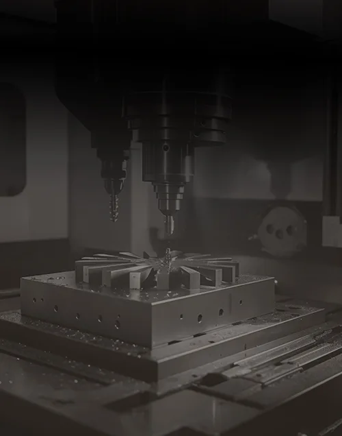 CapabilitiesPrototypes and production partsMechanical ManufacturingMechanical Manufacturing Capability: Excellent Craftsmanship, Creating Exceptional QualityParts Manufacturing and ProcessingParts Manufacturing and Processing: Meticulous Craftsmanship, Creating Premium PartsMaterial Surface FinishesMaterial Surface Finishes: Refining Processes, Reinventing Material ExcellenceInspection and Quality ControlInspection and Quality Control: Precise Control, Quality AssuranceHeat Treatment ServicesHeat Treatment Services: Precise Temperature Control, Reinventing Material ExcellencePrecision AssemblyPrecision Assembly: Meticulous Craftsmanship, Achieving Perfect Combinations
 - Industries
 IndustriesDeveloping revolutionary productsAutomotivePrecision Machining Services for Auto Parts in the Automotive Manufacturing IndustryMedical Equipment & HealthcarePrecision Medical Machining ServicesMilitary and AerospacePrecision Machining Services for Military and Aerospace ManufacturingElectronics and SemiconductorPrecision Machining Services for Electronics and Semiconductor ManufacturingEnergy and Industrial EquipmentPrecision Machining Services for Energy and Industrial Equipment Manufacturing
 - Materials
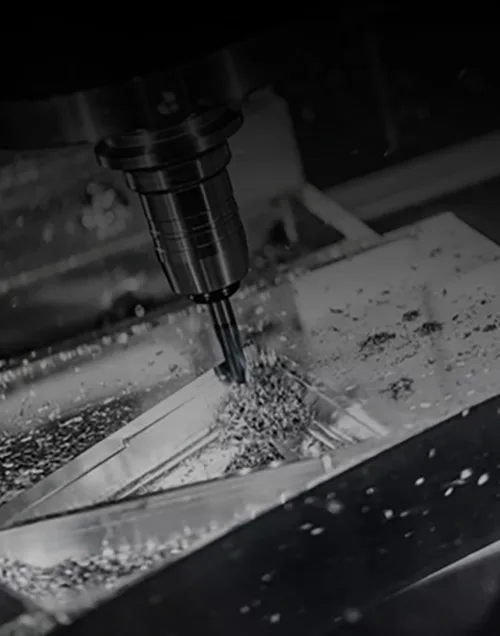 Metal MachiningProtoypes and production partsTitanium Alloy MachiningPrecision CNC Machining of Titanium MaterialsCopper and Aluminum MachiningPrecision CNC Machining of Copper and Aluminum AllStainless SteelMachiningPrecision CNC Machining of Stainless Steel MateriaDie Steel MachiningPrecision CNC Machining of Die Steel MaterialsComposite Material MachiningPrecision CNC Machining of Composite Materials
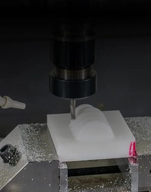 Plastic MachiningProtoypes and production parts
 - About Us
- Blogs